
IN SHORT
- A sharp dip starts here: the dip can only be as sharp as the gold film, about 50 nm thick, smooth and clean.
- Software can’t fix the film: a rough or patchy film scatters light and blurs the dip, and no processing recovers it (TN-04: Where the precision comes from).
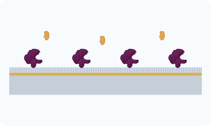
- The same gold carries the coating: it holds the layer that captures your molecules, such as our low-background AffiCoat (TN-06: The binding surface).
Overview
The SPR signal is generated in a gold film roughly 50 nanometres thick. Everything about that film (its thickness, smoothness, purity and how it is held to the glass) shows up later as the depth and width of the resonance, the noise on your baseline and how well your surface chemistry forms.
This note explains what makes a good film, how films are made, what degrades them, and what to look for in a sensor chip.
1 · THE FILM
Why gold, and why about 50 nm
Gold supports a strong plasmon in the visible and near-infrared, does not oxidize in air or buffer, and takes thiol chemistry directly (TN-06: The binding surface). Silver gives a sharper resonance but corrodes.
Thickness matters. Around 50 nm of gold gives the deepest dip, with a narrow width. Thinner films lose too much light into the plasmon, and the dip gets shallow and broad. Thicker films give a narrower but much shallower dip, because too little light reaches the surface.

2 · FILM QUALITY
What makes a good film
Five properties decide how a film performs, and each one shows up in your data when it is off.
The resonance can only be as sharp as the film allows. No software recovers a film that scatters, or a surface that won’t take chemistry evenly. That is why the film is where a lensless instrument cannot cut corners (TN-03: Lensless optics and wavelength readout).
| Property | When it’s right | When it’s wrong, what you see |
|---|---|---|
| Thickness | Uniform, close to target | Shallow or broad dip; differences between channels and between chips |
| Smoothness | Low roughness, fine continuous grains | Light scatters, the dip broadens and shifts; a broad dip is tracked less precisely, so baseline noise goes up (TN-04: Where the precision comes from) |
| Purity | Clean gold, nothing trapped in or on it | Offsets and drift; monolayers form patchily, so coupling yields vary and background binding increases (TN-06: The binding surface) |
| Continuity | No pinholes, islands or voids | Weak or uneven signal; chemistry reaches the glass through the gaps |
| Adhesion | Firmly bonded, with a minimal adhesion layer | Film lifts or blisters during regeneration; a thick adhesion layer damps the plasmon (section 4) |

3 · HOW FILMS ARE MADE
Physical vapour deposition
Sensor-grade gold films are made by physical vapour deposition (PVD): gold is turned into vapour in a high vacuum and condenses on the glass, a few atoms at a time.
The method is only part of the story. What decides the final film is how well the process is run: how clean the substrate is before coating, the vacuum quality, the deposition rate, thickness monitoring, and batch-to-batch consistency. Those are the skills of a specialized coating house, not of a general lab evaporator.
| Method (all PVD) | How it works | Strengths | Watch-outs |
|---|---|---|---|
| Thermal evaporation | Gold heated in a crucible until it evaporates | Simple, pure gold, gentle on the substrate | Rate and thickness control depend on the setup; grain size depends on rate and substrate temperature |
| Electron-beam evaporation | An electron beam melts a small spot of the gold source | High purity, precise rate and thickness control | Needs good vacuum and process control to stay smooth |
| Sputtering | Ions knock gold atoms off a target | Dense, well-adhered films, uniform over large areas | Higher-energy process; can trap gas or roughen the film if not tuned |
| Template stripping (reference) | Gold deposited on an ultra-flat template, then peeled off | Near-atomically flat surfaces | A research technique; not practical for routine sensor chips |
4 · THE ADHESION LAYER
Holding the gold to the glass
Gold does not stick well to glass on its own, so a few nanometres of an adhesion metal, usually chromium or titanium, go down first. That layer has a cost.
It damps the plasmon: adhesion metals absorb light, and weaken and broaden the resonance. The thicker the layer, the bigger the effect. And it can move: chromium and titanium can diffuse through the gold, along the boundaries between grains, and oxidize at the surface. Heat speeds this up. Over time that changes the film’s optical behaviour and the surface your chemistry sees.
So the adhesion layer should be just thick enough to hold the gold, deposited in the same vacuum run, and well controlled from batch to batch.

5 · CLEANING
Cleaning, and what it does to the gold
Cleaning removes organic contamination and old monolayers, but every method also acts on the gold. Plasma cleaning (oxygen or argon) removes organic layers and thiol monolayers efficiently. Oxygen plasma also leaves a thin gold oxide, and a monolayer built on it can trap that oxygen. Aggressive or repeated treatment can roughen the film.
UV-ozone is gentler on the film, but also oxidizes the surface. Strong oxidizing acids clean thoroughly but are hard on thin films and adhesion layers, and are best avoided for routine reuse.
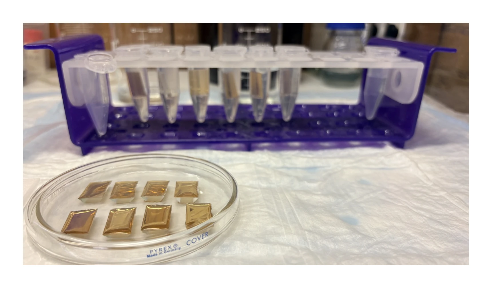
For most users, a fresh, clean chip from a controlled batch is more reproducible than a heavily cleaned one. If you reuse chips, use the gentlest method that works and check the baseline before trusting the surface.
6 · HANDLING
Both faces matter
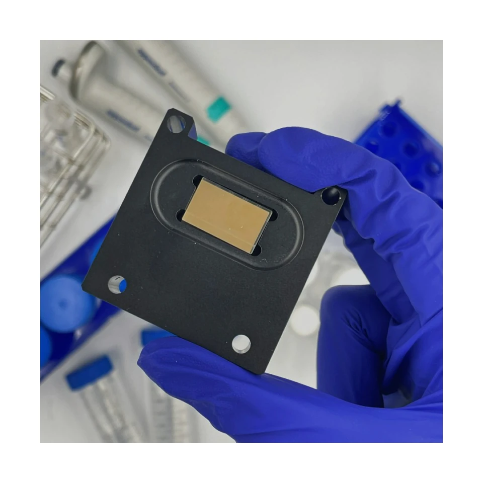
The chip couples optically to the instrument through its back side, so the back side matters as much as the gold. A fingerprint or dust on either face shows up as noise and an offset baseline; a scratch on the gold shows up in every run.
Hold chips by the short edges, and store them clean and dry.
7 · OUR CHIPS
How we source our chips
Our sensor chips are coated by a world-class coating service, to our specification, on Dove-prism substrates made for our instruments. Every chip, and every channel on it, starts from the same optical point, which the lensless design relies on (TN-03: Lensless optics and wavelength readout).
The coating report for a batch is available on request.
Related
TECH NOTE · TN-03
Lensless optics and wavelength readout
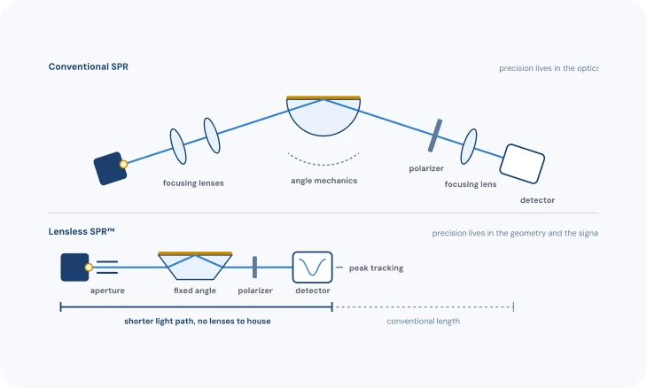
Angle vs wavelength readout, what a conventional optical bench needs, and what the lensless design changed.
TECH NOTE · TN-04
Where the precision comes from
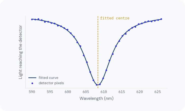
How the dip is located more finely than one pixel, and what sets the smallest shift you can see.
TECH NOTE · TN-06
The binding surface
Surface chemistries, coupling and capture, and how to choose one for your molecule.